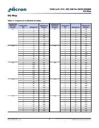
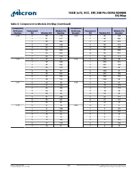
Памяти и накопители Micron 2933 - инструкция пользователя по применению, эксплуатации и установке на русском языке. Мы надеемся, она поможет вам решить возникшие у вас вопросы при эксплуатации техники.
Если остались вопросы, задайте их в комментариях после инструкции.
"Загружаем инструкцию", означает, что нужно подождать пока файл загрузится и можно будет его читать онлайн. Некоторые инструкции очень большие и время их появления зависит от вашей скорости интернета.
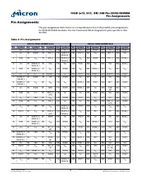
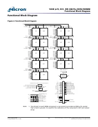

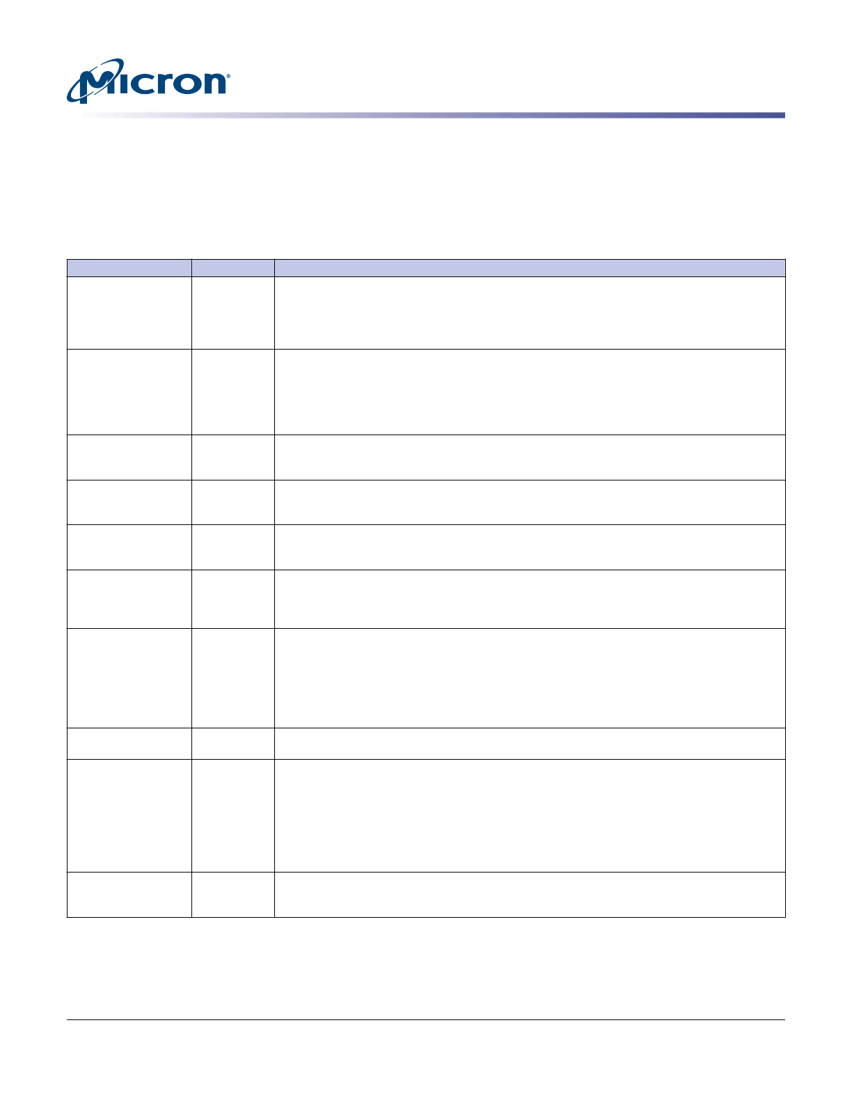
Pin Descriptions
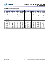
The pin description table below is a comprehensive list of all possible pins for DDR4
modules. All pins listed may not be supported on this module. See Functional Block Di-
agram for pins specific to this module.
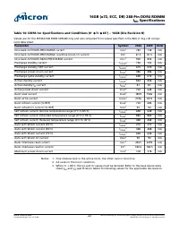
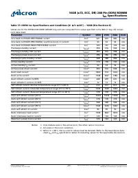
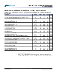
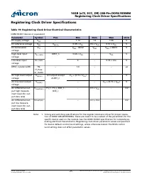
Table 5: Pin Descriptions
Symbol
Type
Description
Ax
Input
Address inputs:
Provide the row address for ACTIVATE commands and the column address for
READ/WRITE commands in order to select one location out of the memory array in the respec-
tive bank (A10/AP, A12/BC_n, WE_n/A14, CAS_n/A15, and RAS_n/A16 have additional functions;
see individual entries in this table). The address inputs also provide the op-code during the
MODE REGISTER SET command. A17 is only defined for x4 SDRAM.
A10/AP
Input
Auto precharge:
A10 is sampled during READ and WRITE commands to determine whether an
auto precharge should be performed on the accessed bank after a READ or WRITE operation
(HIGH = auto precharge; LOW = no auto precharge). A10 is sampled during a PRECHARGE com-
mand to determine whether the precharge applies to one bank (A10 LOW) or all banks (A10
HIGH). If only one bank is to be precharged, the bank is selected by the bank group and bank
addresses.
A12/BC_n
Input
Burst chop:
A12/BC_n is sampled during READ and WRITE commands to determine if burst
chop (on-the-fly) will be performed (HIGH = no burst chop; LOW = burst chopped). See Com-
mand Truth Table in the DDR4 component data sheet.
ACT_n
Input
Command input:
ACT_n defines the ACTIVATE command being entered along with CS_n. The
input into RAS_n/A16, CAS_n/A15, and WE_n/A14 are considered as row address A16, A15, and
A14. See Command Truth Table.
BAx
Input
Bank address inputs:
Define the bank (with a bank group) to which an ACTIVATE, READ,
WRITE, or PRECHARGE command is being applied. Also determine which mode register is to be
accessed during a MODE REGISTER SET command.
BGx
Input
Bank group address inputs:
Define the bank group to which a REFRESH, ACTIVATE, READ,
WRITE, or PRECHARGE command is being applied. Also determine which mode register is to be
accessed during a MODE REGISTER SET command. BG[1:0] are used in the x4 and x8 configura-
tions. x16-based SDRAM only has BG0.
C0, C1, C2
(RDIMM/LRDIMM on-
ly)
Input
Chip ID:
These inputs are used only when devices are stacked; that is, 2H, 4H, and 8H stacks for
x4 and x8 configurations using through-silicon vias (TSVs). These pins are not used in the x16
configuration. Some DDR4 modules support a traditional DDP package, which uses CS1_n,
CKE1, and ODT1 to control the second die. All other stack configurations, such as a 4H or 8H,
are assumed to be single-load (master/slave) type configurations where C0, C1, and C2 are used
as chip ID selects in conjunction with a single CS_n, CKE, and ODT. Chip ID is considered part of
the command code.
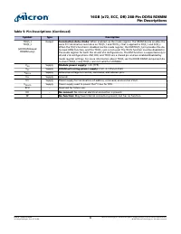
CKx_t
CKx_c
Input
Clock:
Differential clock inputs. All address, command, and control input signals are sampled
on the crossing of the positive edge of CK_t and the negative edge of CK_c.
CKEx
Input
Clock enable:
CKE HIGH activates and CKE LOW deactivates the internal clock signals, device
input buffers, and output drivers. Taking CKE LOW provides PRECHARGE POWER-DOWN and
SELF REFRESH operations (all banks idle), or active power-down (row active in any bank). CKE is
asynchronous for self refresh exit. After V
REFCA
has become stable during the power-on and ini-
tialization sequence, it must be maintained during all operations (including SELF REFRESH). CKE
must be maintained HIGH throughout read and write accesses. Input buffers (excluding CK_t,
CK_c, ODT, RESET_n, and CKE) are disabled during power-down. Input buffers (excluding CKE
and RESET_n) are disabled during self refresh.
CSx_n
Input
Chip select:
All commands are masked when CS_n is registered HIGH. CS_n provides external
rank selection on systems with multiple ranks. CS_n is considered part of the command code
(CS2_n and CS3_n are not used on UDIMMs).
16GB (x72, ECC, DR) 288-Pin DDR4 RDIMM
Pin Descriptions
CCMTD-1725822587-9899
asf18c2gx72pdz.pdf - Rev. H 7/19 EN
6
Micron Technology, Inc. reserves the right to change products or specifications without notice.
© 2015 Micron Technology, Inc. All rights reserved.
Характеристики

Остались вопросы?Не нашли свой ответ в руководстве или возникли другие проблемы? Задайте свой вопрос в форме ниже с подробным описанием вашей ситуации, чтобы другие люди и специалисты смогли дать на него ответ. Если вы знаете как решить проблему другого человека, пожалуйста, подскажите ему :)


