Памяти и накопители Micron 2933 - инструкция пользователя по применению, эксплуатации и установке на русском языке. Мы надеемся, она поможет вам решить возникшие у вас вопросы при эксплуатации техники.
Если остались вопросы, задайте их в комментариях после инструкции.
"Загружаем инструкцию", означает, что нужно подождать пока файл загрузится и можно будет его читать онлайн. Некоторые инструкции очень большие и время их появления зависит от вашей скорости интернета.
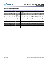
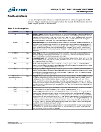
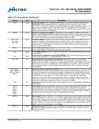
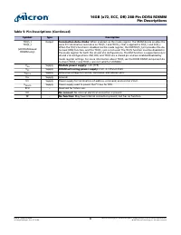
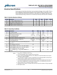
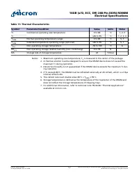

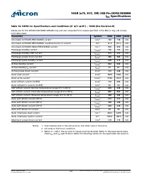
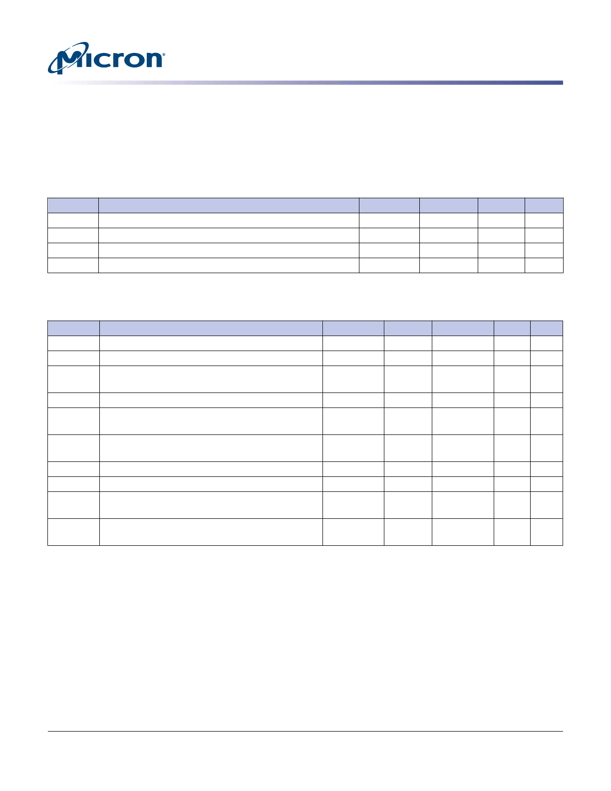
Electrical Specifications
Stresses greater than those listed may cause permanent damage to the module. This is a
stress rating only, and functional operation of the module at these or any other condi-
tions outside those indicated in each device's data sheet is not implied. Exposure to ab-
solute maximum rating conditions for extended periods may adversely affect reliability.
Table 9: Absolute Maximum Ratings
Symbol Parameter
Min
Max
Units
Notes
V
DD
V
DD
supply voltage relative to V
SS
–0.4
1.5
V
V
DDQ
V
DDQ
supply voltage relative to V
SS
–0.4
1.5
V
V
PP
Voltage on V
PP
pin relative to V
SS
–0.4
3.0
V
V
IN
, V
OUT
Voltage on any pin relative to V
SS
–0.4
1.5
V
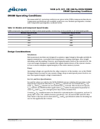
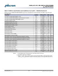
Table 10: Operating Conditions
Symbol Parameter
Min
Nom
Max
Units Notes
V
DD
V
DD
supply voltage
1.14
1.20
1.26
V
V
PP
DRAM activating power supply
2.375
2.5
2.75
V
V
REFCA(DC)
Input reference voltage –
command/address bus
0.49 × V
DD
0.5 × V
DD
0.51 × V
DD
V
I
VTT
Termination reference current from V
TT
–750
–
750
mA
V
TT
Termination reference voltage (DC) –
command/address bus
0.49 × V
DD
-
20mV
0.5 × V
DD
0.51 × V
DD
+
20mV
V
I
IN
Input leakage current; any input excluding ZQ; 0V <
V
IN
< 1.1V
–5
–
5
µA
I
ZQ
Input leakage current; ZQ
–50
–
10
µA
I
OZpd
Output leakage current; V
OUT
= V
DD
; DQ is High-Z
–
–
10
µA
I
OZpu
Output leakage current; V
OUT
= V
SS
; DQ is High-Z;
ODT is disabled with ODT input HIGH
–50
–
–
µA
I
VREFCA
V
REFCA
leakage; V
REFCA
= V
DD
/2 (after DRAM is ini-
tialized)
–4.5
–
4.5
µA
Notes: 1. V
DDQ
balls on DRAM are tied to V
DD
.
2. V
PP
must be greater than or equal to V
DD
at all times.
3. V
REFCA
must not be greater than 0.6 × V
DD
. When V
DD
is less than 500mV, V
REF
may be
less than or equal to 300mV.
4. V
TT
termination voltages in excess of specification limit adversely affect command and
address signals' voltage margins and reduce timing margins.
5. Command and address inputs are terminated to V
DD
/2 in the registering clock driver. In-
put current is dependent on termination resistance set in the registering clock driver.
6. Tied to ground. Not connected to edge connector.
7. Multiply by the number of module ranks and then times the number of die per package.
8. RCD input current
16GB (x72, ECC, DR) 288-Pin DDR4 RDIMM
Electrical Specifications
CCMTD-1725822587-9899
asf18c2gx72pdz.pdf - Rev. H 7/19 EN
16
Micron Technology, Inc. reserves the right to change products or specifications without notice.
© 2015 Micron Technology, Inc. All rights reserved.
Характеристики

Остались вопросы?Не нашли свой ответ в руководстве или возникли другие проблемы? Задайте свой вопрос в форме ниже с подробным описанием вашей ситуации, чтобы другие люди и специалисты смогли дать на него ответ. Если вы знаете как решить проблему другого человека, пожалуйста, подскажите ему :)


